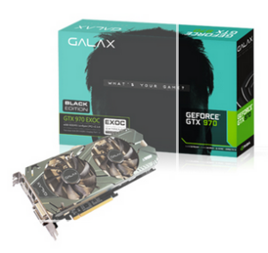
 We received our first GTX 970, the EXOC Black Edition from GALAX, at the very end of December, and we have been testing it against a recently purchased reference version of the 290X from VisionTek, as well as against our original non-throttling mildly overclocked PowerColor 290X PCS+. We have had a couple of extra weeks with our GALAX GTX 970 EXOC, which is more than usual as we attempted to investigate its memory controller whose specifications have recently been downgraded by Nvidia.
We tested our GALAX GTX 970 EXOC at factory-clocked speed, stock, and further overclocked, against the R9 290X and against the GTX 980, with 28 games at 2560×1600 and at 1920×1080 with the demanding settings that gamers use. We wanted to especially see if we could find any practical issues with the GTX 970’s memory controller which was respecified with a lower number of ROPs, less Cache, and downgraded from having a full 4.0GB of VRAM, to having a 4GB framebuffer with 3.5GB of fast access VRAM, plus 0.5GB with much slower access.
The Corrected Specifications of the GTX 970 and Nvidia’s apology
Very little has actually changed regarding the GTX 970 specifications since it launched in September, and since its overstated specification issues were brought to light about three weeks ago. Like the GTX 980 and the R9 290X, the GTX 970 comes equipped with 4GB of fast GDDR5 video memory (vRAM). Unlike the GTX 980 and the 290X, the GTX 970 uses a memory controller which primarily addresses 3.5GB, and secondarily accesses 0.5GB of vRAM much more slowly because of shared resources.
Nvidia’s technical marketing team members claimed that they were originally unaware of their Maxwell architecture’s ability to individually disable ROPs. This meant that the actual ROP count, was originally misrepresented as 64 instead of 56, and the L2 cache was given as 2MB instead of the correct 1.75MB. Nvidia was quick to apologize and to give us a detailed look at the GTX 970’s memory controller.
The difference with the original overstated ROP count is because of limitations with the memory controller’s crossbar. The crossbar routes the data from the processing clusters to the memory controller using the L2 cache. By limiting the L2 cache to 1.75MB, Nvidia had to disable access to the GTX 970’s cache for one of the eight controllers by routing it to another memory controller’s cache which makes it slower for that controller. The original bandwidth specification of 224GB/s was properly lowered to 196 GB/s by Nvidia.
The memory is divided into two parts – one with 3.5GB of the vRAM composed of memory controllers with direct access to the L2 cache – and into a second 0.5GB part sharing access to the cache with another memory controller. A game can only access one section of the vRAM at a time – either it will access the 3.5GB block or the 0.5GB block, but not simultaneously. However, if both segments are being read simultaneously, there will be a noticeable decline in performance compared to the GTX 980’s memory controller which has no such limitations. However, Nvidia said that they designed the GTX 970 to work around these issues with drivers, and when these rare situations happened at extreme resolutions, the performance hit would only be 1-4% compared with the GTX 980’s controller.
When Nvidia published the original specifications, they neglected to give these important details to the reviewers as they have done in the past with other hybrid GTX memory controllers. Technically, Nvidia was correct in stating that the GTX 970 ships with 4GB of vRAM, but they did not give full disclosure.
The issues with “false advertising” primarily rose when Nvidia misstated the number of ROPs as 64 when there are actually 56. However, this technical misstatement does not affect the bandwidth nor the performance of the GTX 970 as it is unable to utilize the full 64 ROPs anyway, due to the limited amount of pixels the shaders send to the ROPs per clock cycle. The GTX 970 is already bottlenecked when it comes to fill rates, unlike with the GTX 980, because for basic pixel operations the GTX 970 is primarily bound by its lower SMM count.
This diagram that Nvidia provided to us and to the other Tech Editors last week shows the correct way in which the GTX 970 accesses its memory.
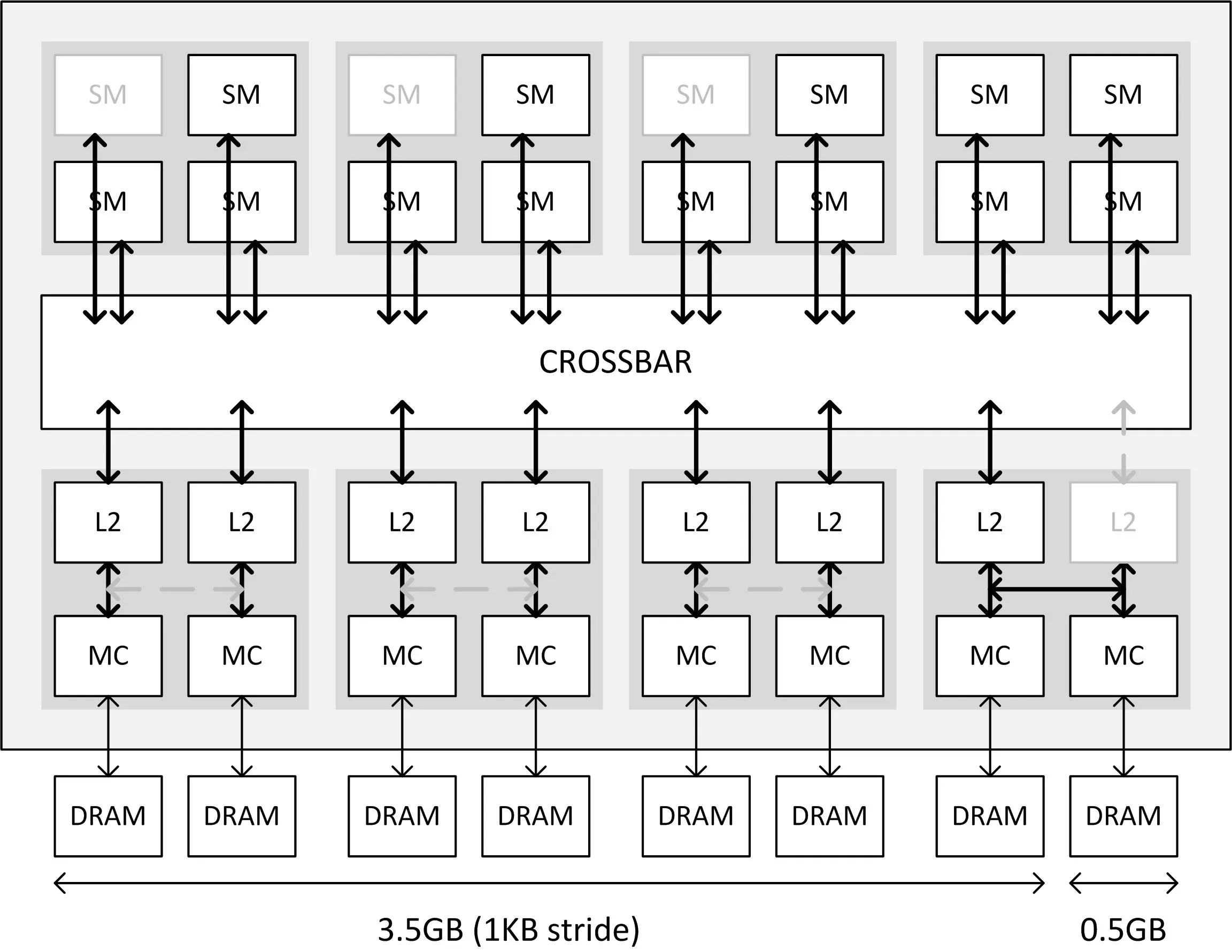
The L2 cache was originally misstated as 2MB but it is actually 1.75MB, and it has been corrected along with number of the ROPs, the bandwidth figures have been downgraded, and the memory controller has been explained in the updated technical specifications, and the GTX 970 Reviewer’s Guide has also been revised.
The Forum Angst and the AMD Advocates
AMD’s army of Advocates certainly have seized on this issue, roundly condemning Nvidia for what their own company has practiced in the past. In one case, AMD overstated the transistor count for Bulldozer’s FX-8150 by 800 million although it actually has only 1.2 billion and not 2 billion as was originally published months earlier; and in another, when they told the reviewers the week of its launch that the HD 6990’s overclock BIOS was covered under warranty, and then they changed their minds a few days after the reviews were published.
Nvidia admitted to their “miscommunication” but insists that the GTX 970 is still the same card with what they call incredible performance for the price, and they have even assisted dissatisfied buyers of the GTX 970 to return, refund, and/or upgrade their card even if the upgrade period normally allowed by resellers had expired. Yet, three weeks later, the tech forums are still buzzing with tech posters posting the same inflammatory and negative comments about Nvidia’s “deceit”.
The Nvidia GeForce forums have exploded with angry comments all over the world. In the USA, there are three hundred pages on this single topic that would make it seem to be a PR catastrophe for Nvidia. Yet the worldwide petition to force Nvidia to refund money to GTX 970 buyers has no traction. Less than 6,000 people signed – out of hundreds of thousands of GTX 970 owners!
Looking closely at the anti-GeForce threads, one thing becomes very clear – you will see the same pictures, the same names, and the same users posting their anger over and over and over again – basically the same posters posting in multiple threads across many tech forums. If they had any sense and are really legitimate owners of the GTX 970, one wonders why they haven’t refunded their GTX 970s by now if they are really as angry as they claim to be.
So where does this negativity and anti-Nvidia sentiment come from? One can only assume that AMD’s army of thousands of “Advocates” are at work. It appears that AMD’s “targeted” marketing to Social Media which began over 6 years ago under former CMO Nigel Dessau is largely a failure in influencing buying decisions although it has negatively impacted our tech communities.
Real World Gaming and the GTX 970
Does the GTX 970’s new limitations actually impact performance in games? According to Nvidia, the maximum performance hit for rare situations where the 0.5GB of memory is accessed in games is minimal – only up to about 4% even at 4K and with maximum details turned on. The GTX 970 is designed to split its memory buffer this way and Nvidia says the card is working exactly as intended..
We went looking for these problems with the GTX 970 versus the GTX 980 (and versus the R9 290X) in several ways. We tested the GTX 970 against the GTX 980 and attempted to find problematic games that would stress the two memory controllers simultaneously.
Besides testing with 28 games, we focused on benching several of the console ports that use a lot of video memory like Middle Earth: Shadows of Mordor, BF4 ,and Dragon’s Age; Inquisition. The GTX 970 may take a slightly larger hit in certain circumstances than the GTX 980 but when you are in situations where the 0.5 GB limited memory controller access begins to affect performance, you are already in unplayable situations for both cards.
Our conclusion: At 2560×1600, and at even higher 4K resolutions with DSR applied, we could not find a single situation where the memory controller affected the framerates where they were not already too low for game play. Perhaps GTX 970 SLI might have some issues, but that testing is beyond the scope of this evaluation.
What we now really want to see is the GTX 970’s performance – in the form of stock clocks, at GALAX EXOC clocks +76MHz offset over reference, and overclocked as far as we can go on stock voltage and fan profile. And we want to compare its performance with the GTX 980 and with its main competitor, the R9 290X, which is priced similarly to the GTX 970. Of course, we shall also give you our “Big Picture” to place the GTX 970 into a line up with 7 other AMD and Nvidia cards.
First, lets unbox the GALAX GTX 970 EXOC and look at it specifications and features:
The GALAX GTX 970 EXOC Black Editioin is an exciting card that launched in mid-September last year, about the same time that GALAX merged from Galaxy and KFA2. The GTX 970 EXOC is built with the latest Maxwell GPU architecture to deliver more performance with double the efficiency of previous generations, while also featuring an aggressive factory overclock, enhanced PCB design, and a superior custom cooler.
The GALAX GTX 970 EXOC Black Edition is a good looking black and gray card that features a 11% overclock over stock speeds with its factory overclock guaranteed to reach 1317MHz.
Unboxing the GALAX GTX 970 EXOC Black Edition
The GALAX GTX 970 EXOC Black Edition arrives in a box that advertises the card without its specifications, other than it is a “GeForce GTX 970 EXOC”. We also learn that EXOC stands for “Extreme Overclock” and that it features 6- plus 8-pin PCIe 3.0, its 4GB framebuffer, dual-link DVI, Display Port 1.2, and HDMI connectors. The box also features Nvidia’s GameStream, GameWorks, G-sync, and DX12, as well as a new slogan – “What’s Your Game?”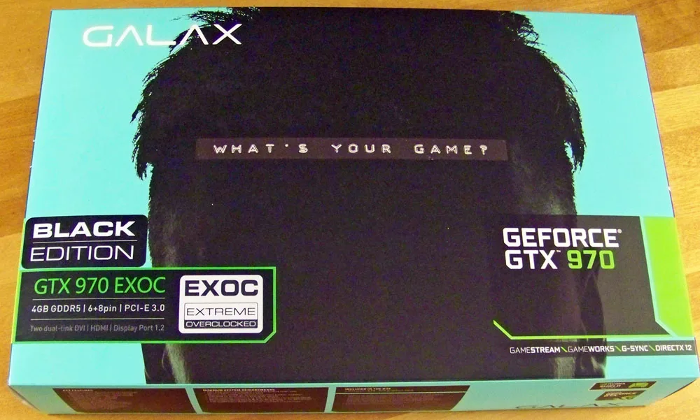
The back of the GALAX box goes into more details and shows exactly what is included with the card. Surround, SLI, PhysX and 3D Vision are featured also on the box, along with performance for up to 4K resolutions.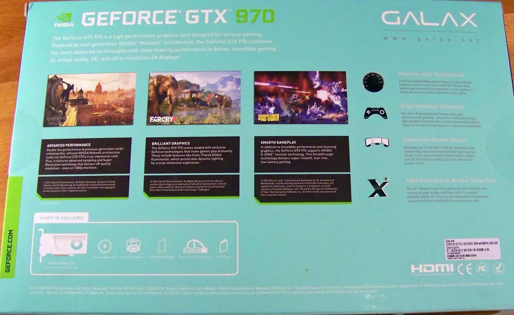
Great utilities are included, including GALAX’s Xtreme Tuner Plus which includes an improved GPU voltage tuner. One end panel shows the card’s key features and minimum system requirements (500W PSU).
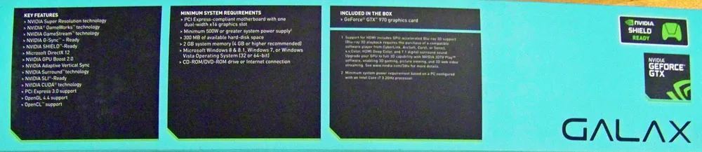 The end panels gives the key features, minimum system requirements as well as what’s included in the box. The card comes well-protected and in an anti-static bag.
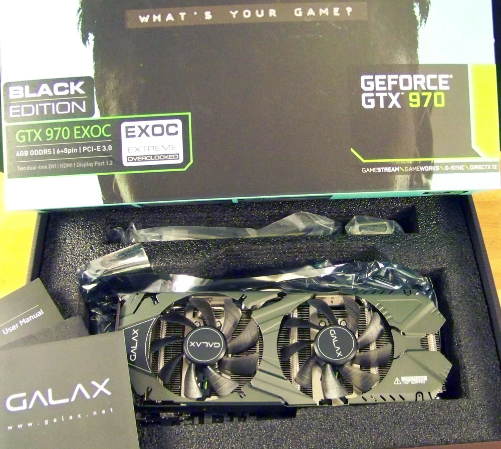
Inside the box, besides the new GALAX GTX 970 EXOC, we find a driver CD, manual, two molex to PCIe connectors, a DVI to DVI connector, and warranty service information. GALAX thoughtfully included an 8-pin molex adapter, a first for this reviewer who is only used to seeing 6-pin adapters.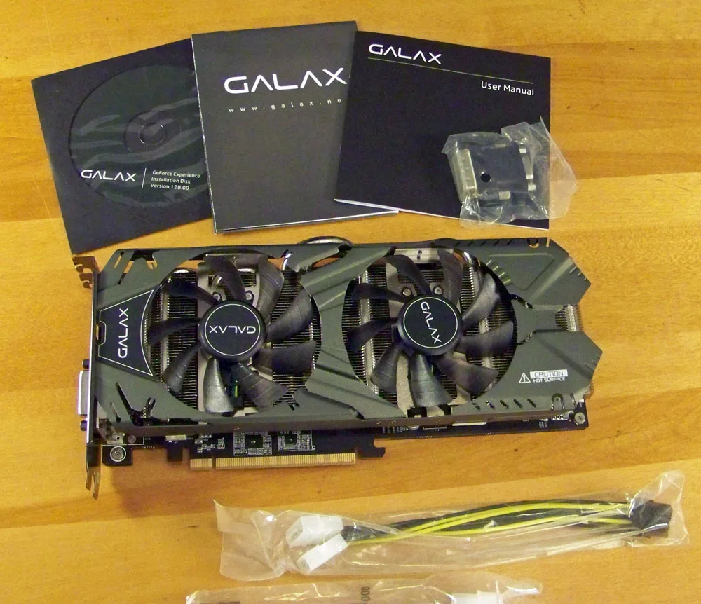
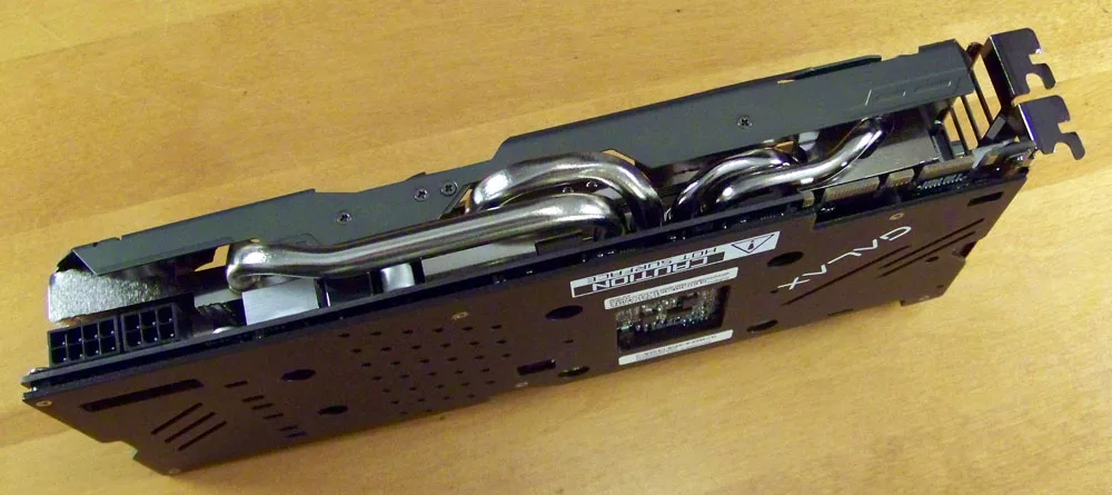
The GALAX GTX 970 EXOC is on a relatively small PCB with two very large quiet-running fans and a beefy cooler to keep the GPU cool.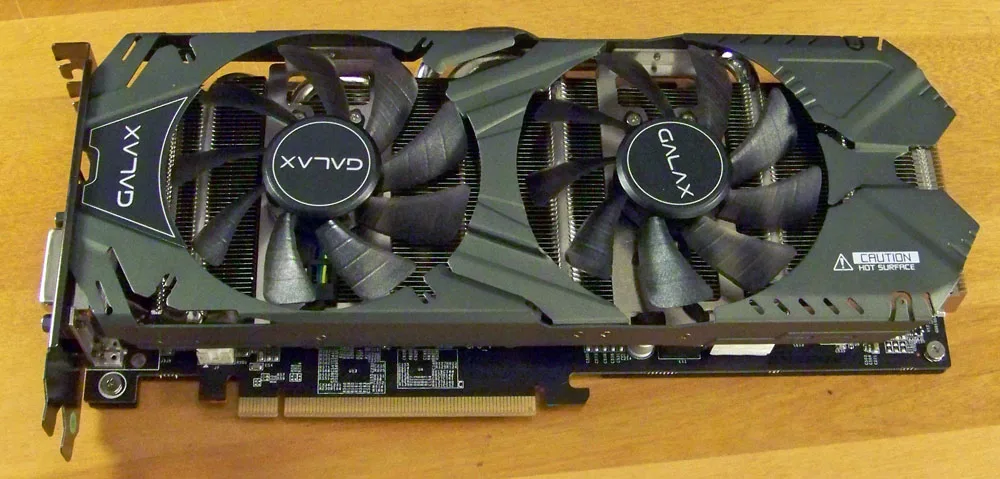
Another angle shows the 6-pin plus 8-pin PCIe connectors which are an upgrade over two 6-pin connectors. It should be useful for overclocking.
The connectors include 2 dual-link DVI, DisplayPort 1.2, and HDMI.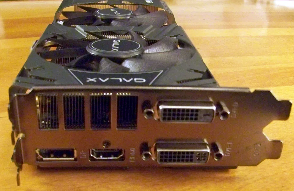
Let’s turn it over. It uses GALAX’ custom design to maximize the cooling over the entire video card and the backplate makes it look better as well as cool better.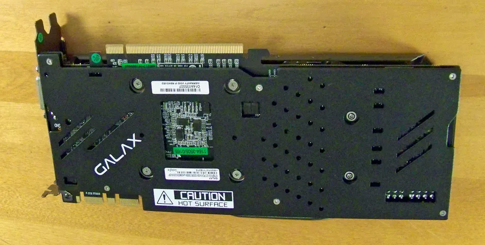 The GALAX GTX 970 EXOC video card is warrantied for three years. GALAX has included their Xtreme Tuner overclocking software on the driver CD or as a download on their site and you can even raise the voltage.
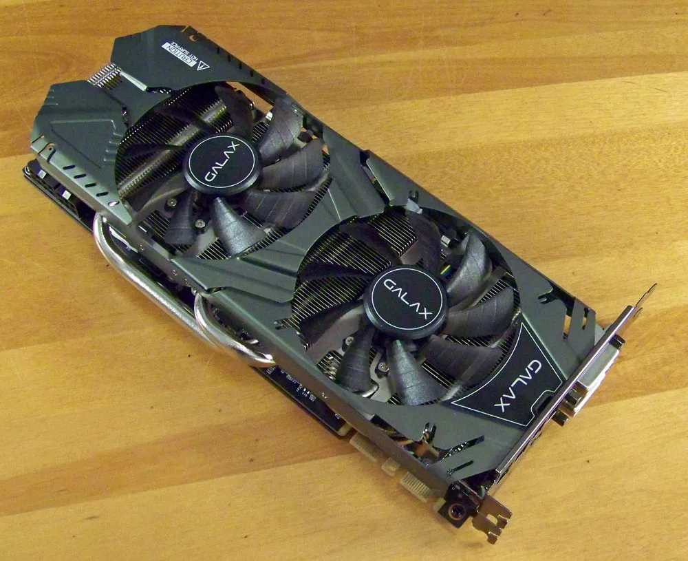
The GALAX GTX 970 EXOC looks like a great card. l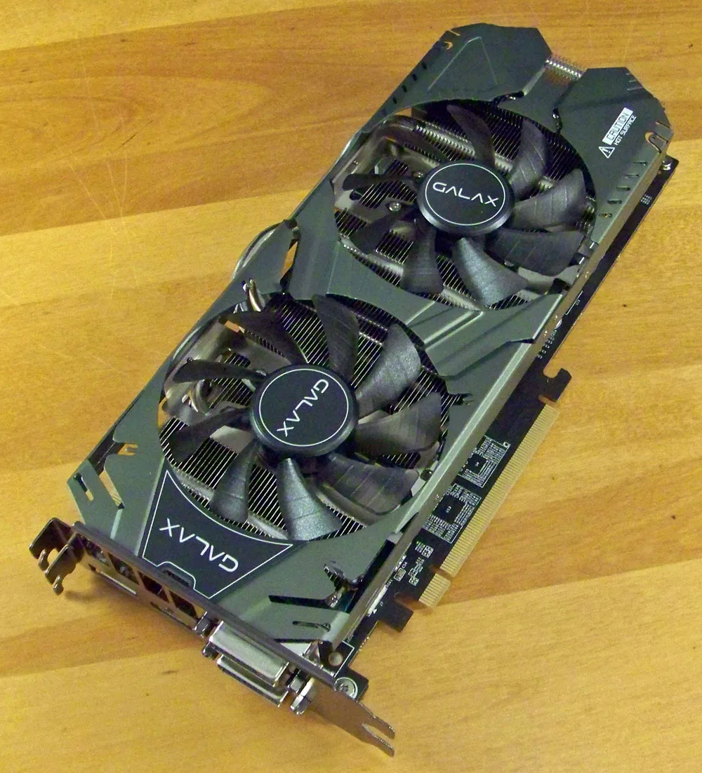 Above we see it from another angle.
We can’t wait to test out our new card but let’s look at the competition.
The GALAX GTX 970 EXOC’s Competition – the R9 290X – and the ongoing myth of the “throttling” Reference version (now)
We will compare performance to price as the reference and overclocked GTX 970s are generally priced starting at $329 at Newegg to near $400, while the GALAX GTX 970 EXOC Black Edition sells for $349 from the GALAX Store which puts it in the midst of the overclocked GTX 970s price-wise. The GALAX GTX 970 which is clocked at reference speeds is priced at $329.99 but is out of stock currently.
AMD’s R9 290X SKUs are generally priced beginning from $299 to well over $400 at Newegg.com. The overclocked versions are generally clocked from 1030MHz to 1050MHz on the core, up 30 MHz to 50MHz over reference, same as our PowerColor clocked PCS+ 290X. At the time of writing, only one reference version of the 290X is available at Newegg.
The reference versions are evidently quite unpopular, largely from getting a bad reputation for running hot and throttling well below AMD’s “up to 1000MHz” on the core when it first came out. We were quite fortunate to get a PowerColor PCS+ overclocked reference version of the 290X at launch from retail that is clocked at 1030MHz on the core and it does not throttle in cool ambient temperatures. And in testing our recently purchased VisionTek reference version which runs at 1000MHz, we find it does not throttle significantly either. You will be able to see the scaling between the two 290Xes which are clocked 30MHz apart.
Evidently the early Hawaii GPUs at their launch barely met specifications as the reference cooler was unable to cool them properly without throttling the clock speeds. AMD was determined to beat the original TITAN’s performance even if it meant running the 290X on the edge with the Uber clocks.
The later Hawaii GPUs evidently have no such issues with the reference cooler as long as the gamer is willing to put up with what most consider excessive noise from a fan that spins up to 55% when the GPU hits 95C. This is a rather big issue that CrossFire users face when picking a 290/X video card – either use reference and put up with extreme noise from two cards, or use an open design for two hot-running cards and roast the interior of your case and the PC hardware inside. Of course, the ideal solution is to use water to cool two hot-running Hawaii GPUs, but even a highly overclocked watercooled R9 290X will not catch a less expensive aftermarket air cooled GTX 980 in performance.
GALAX GTX 970 Features
Let’s look at the GALAX GTX 970 EXOC specifications from the GALAX store:
The GALAX GeForce GTX 970 EXOC Black Edition is a high performance graphics card designed for serious gamers, produced in a black PCB, anodized aluminum black backplate, with a 1317 MHz factory overclock, powered by the next generation NVIDIA® Maxwell architecture.
-
1317 MHz factory overclock
-
Black PCB
-
Anodized Aluminum Black Backplate protects and cools components and reinforces PCB
-
All new Silence Extreme cooler reduces temps by up to 10C
-
Silence Extreme technology switches to single fan cooling at idle for almost noiseless operation
-
Quad mixed-gauge heat pipes ensure maximum heat dissipation
-
Copper base with solid aluminum cover
-
5 + 2 Phase enhanced power system with 8 + 6-pin inputs delivers up to 50% more power for overclocking, can support up to 225w
-
NVIDIA® Dynamic Super Resolution (DSR)
-
NVIDIA® Global Illumination (VXGI)
-
NVIDIA® GameWorks Technology
-
NVIDIA® GameStream Technology
-
NVIDIA® TXAA Technology
-
NVIDIA GPU Boost 2.0
-
NVIDIA PhysX® Technology
-
NVIDIA FXAA Technology
-
NVIDIA Adaptive Vertical Sync
-
NVIDIA Surround
-
Support for four concurrent displays including: Two dual-link DVI, HDMI and DisplayPort 1.2
-
Microsoft DirectX 12
-
NVIDIA® 3D Vision® Ready
-
NVIDIA SLI® Ready Technology
-
NVIDIA CUDA® technology
-
PCI Express 3.0 support
-
OpenGL 4.4 support
-
OpenCL support
-
NVIDIA SHIELD Ready
-
NVIDIA GSYNC Ready
FEATURES of the GALAX GTX 970 EXOC
| GPU Engine Specs: | |
| CUDA Cores | 1664 |
| Base Clock (MHz) | 1164 |
| Boost Clock (MHz) | 1317 |
| Memory Specs: | |
| Memory Speed | 3505 (7010 ) Mhz |
| Standard Memory Config | 4096MB |
| Memory Interface Width | 256-bit GDDR5 |
| Memory Bandwidth (GB/sec) | 224 |
| Feature Support: | |
| OpenGL | 4.4 |
| Bus Support | PCI-E 3.0 |
| Certified for Windows 8 | Yes |
| Supported Technologies | DirectX 12 |
| SLI Options | 3-WAY |
| Display Support: | |
| Multi Monitor | 4 |
| Maximum Digital Resolution | 4096×2160 |
| Maximum VGA Resolution | 2048×1536 |
| HDCP | Yes |
| HDMI | Yes |
| Standard Display Connectors | Dual DVI-I/DVI-D, HDMI x1, DisplayPort 1.2 x1 |
| Audio Input for HDMI | Internal |
| Standard Graphics Card Dimensions: | |
| Length | 271 mm |
| Height | 124.3 mm |
| Width | 41.5 mm |
| Power Specs: | |
| Maximum Graphics Card Power (W) | 145W |
| Minimum System Power Requirement (W) | 500W |
| Supplementary Power Connectors | One 6-pin,One 8-pin |
| Model: | |
| Product Code | 97NQH6DNB4TX |
| UPC Code | 4895147118215 |
| Warranty: | 3 year extended warranty when registered online within 30 days (2 year standard warranty) |
System Requirements
-
PCI Express-compliant motherboard with one dual-width x 16 graphics slot
- 1 x 6-pin, 1 x 8pin PCI Express supplementary power connectors
- Minimum 500W or greater system power supply (with a minimum 12V current rating of 42A)
- 300MB of available hard-disk space
- 2GB system memory (4GB or higher recommended)
- Microsoft Windows 8 & 8.1, Windows 7, Windows Vista (32 or 64-bit)
-
Internet connection
The specifications looks great, the 3-year warranty is premium, and the price is right. Let’s head for the test configuration before we chart the benchmark results.
Test Configuration – Hardware
Test Configuration – Hardware
- ASUS Z97-E motherboard (Intel Z97 chipset, latest BIOS, PCIe 3.0 specification, CrossFire/SLI 8x+8x)
- Intel Core i7-4790K (reference 4.0GHz, HyperThreading and Turbo boost is on to 4.4GHz; DX11 CPU graphics), supplied by Intel.
- Kingston 16 GB HyperX Beast DDR3 RAM (2×8 GB, dual-channel at 2133MHz, supplied by Kingston)
- GeForce GTX 980, 4GB reference clocks, supplied by Nvidia
- GeForce GTX 970 EXOC Black Edition, 4GB and clocked down to reference clocks, supplied by GALAX
- GeForce GTX 790, reference clocks, supplied by Nvidia
- ASUS STRIX GTX 960 OC Direct CU II, 2GB at ASUS factory overclocked and further overclocked, supplied by ASUS/Nvidia under NDA
- EVGA GTX 660 SOC, downclocked to reference clocks, supplied by Nvidia
- VisionTek R9 280X, reference clocks, supplied by VisionTek
- VisionTek R9 290X, reference clocks; Uber BIOS
- PowerColor R9 290X PCS+, overclocked version +1030MHz; Uber BIOS
- Two 2TB Toshiba 7200 rpm HDDs
- Corsair CX750M, 750W power supply unit
- Cooler Master Seidon240 CPU watercooler, supplied by Cooler Master
- Onboard Realtek Audio
- Genius SP-D150 speakers, supplied by Genius
- Thermaltake Overseer RX-I full tower case, supplied by Thermaltake
- ASUS 12X Blu-ray writer
- HP LP3065 2560×1600 30″ LCD display
Test Configuration – Software
- Nvidia GeForce 347.09 WHQL drivers for GTX 980, and GeForce 347.25 WHQL drivers for all of the other GeForce Cards tested. High Quality, prefer maximum performance, single display. Windows 7 64-bit; very latest updates
- Radeon “Omega” Catalyst 14-12 drivers used for the VisionTek R9 280X and for both of the R9 290Xes. Surface format optimizations, off; Application decide, VSYNC forced off, High Quality, and Tessellation App decide.
- Latest DirectX
- All games are patched to their latest versions.
- VSync is off in the control panel.
- AA enabled as noted in games; all in-game settings are specified with 16xAF always applied; 16xAF forced in control panel for Crysis.
- All results show average, minimum and maximum frame rates except as noted.
- Highest quality sound (stereo) used in all games.
- Windows 7 64, all DX10 titles were run under DX10 render paths; DX11 titles under DX11 render paths.
- GALAX Xtreme Tuner Plus overclocking utility
- EVGA PrecisionX 16
The 28 PC Game benchmarks & 2 synthetic benchmark tests
- Synthetic
- Firestrike – Extreme/Ultra
- Heaven 4.0
DX9- The Witcher 2
- Borderlands 2
DX10- Crysis
DX11- STALKER, Call of Pripyat
- Max Payne 3
- the Secret World
- Sleeping Dogs
- Hitman: Absolution
- Tomb Raider: 2013
- Crysis 3
- BioShock: Infinite
- Metro: Last Light Redux 2014 edition
- Battlefield 4
- Splinter Cell: Blacklist
- ArmA 3
- Total War: Rome II
- Batman: Arkham Origins
- Thief
- Sniper Elite 3
- Watch_Dogs
- GRID: Autosport
- Middle Earth: Shadows of Mordor
- Alien Isolation
- Assassin’s Creed Unity
- Civilization Beyond Earth
- Far Cry 4
- Dragon’s Age: Inquisition
- The Crew
Before we get to the GALAX GTX 970 performance charts, let’s look at overclocking, power draw and temperatures.
Overclocking, Power Draw & Temperatures
Thanks in part to Maxwell’s power efficiency, the GeForce GTX 970 evidently has reasonable headroom for overclocking. The GeForce GTX 970 ships with base clock speeds at 1050MHz. The typical Boost Clock speed is 1178MHz. The Boost Clock speed is based on the average GeForce GTX 970 card running a wide variety of games and applications. And of course, the actual Boost clock will vary slightly from card to card and from game-to-game, depending on actual system conditions. GeForce GTX 970’s memory speed is 7000MHz data rate.
The GeForce GTX 970 reference board measures 10.5” in length. Display outputs include one dual-link DVI, one HDMI and three DisplayPort connectors. Two 6-pin PCIe power connectors are required for operation. The GALAX GTX 970 EXOC Black Edition sports two DVI posts, one HDMI and a DP connection.
Overclocking, Power Draw, Noise and Temperatures
Overclocking the GALAX GTX 970 EXOC is just as easy as overclocking any other GTX 900 or 700 series card. Our GALAX GTX 970 EXOC is already overclocked +76MHz over the Nvidia reference clocks. We were able to overclock a further +90MHz with complete stability even though we did not adjust the voltage nor our fan profile. We also managed +250MHz offset on the memory clocks.
Our maximum observed stock boost was 1430MHz which increased to 1529MHz, typically from 1517MHz to 1529MHz, when we overclocked its core a further 90MHz. Temperatures were very good with 73C as the maximum observed temperature. With the fan profile at automatic, the Galaxy GTX 970 EXOC remained quiet, the fan never exceeding 2500rpm. Even with overclocking further, temperatures generally stayed below 73C and the fan never exceeded 3000rpm. Because of it’s custom fan design, the GALAX GTX 970 EXOC is a quiet card, noticeably quieter than the 290X at any fan speed.
For our testing of the GALAX GTX 780 EXOC, we usually move the temperature target to its maximum 95C and the power target also to its maximum. The power adjustments are slightly higher than for the reference version. In this way, we do not allow lack of power nor moderate temperatures to throttle performance. Likewise, we also max the PowerTune slider for AMD cards.
Although the performance between Maxwell and Hawaii are similar, the power draw is not. The only difference between these two systems is the one on the left (which peaked at 303W) has a the factory overclocked GALAX GTX 970 EXOX running Battlefield 4, and the one on the right (which peaked at 391W), has a stock R9 290X running the same scene.
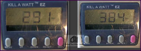
We are not pretending that our power draw tests are “scientific”, or even precise, but they do illustrate that Maxwell is significantly more power efficient than Hawaii and you will use less electricity using the Nvidia card. Since the 290X has more heat to dissipate, the reference 290X cooling fan has to run much faster and will generate more noise that when it was used originally for the HD 79×0 series.
Note: All of our benching was done in the “Uber” BIOS mode so both 290Xes did not throttle as the fan was allowed to ramp up noisily to 55%.
Let’s head to the performance charts to see how the GALAX GTX 970 EXOC Black Edition compares with the reference GTX 980 and fits into Nvidia’s lineup, as well as compare with the R9 290X and with the other video cards for our Big Picture.
Performance summary charts & graphs
Here are the summary charts of 28 modern PC games and 2 synthetic tests. The highest settings are generally chosen and it is DX11 when there is a choice; DX10 is picked above DX9, and the settings are generally ultra or maxed unless specified on the chart. Specific settings are listed on the Main Performance chart. The benches are run at 1920×1200 and at 2560×1600.
The 290X versus the GTX 970
Here we see just a stock clocked GTX 970 versus the reference (non-throttling, Uber) 290X. Wins are bolded and if there is a tie, both results are given in Bold.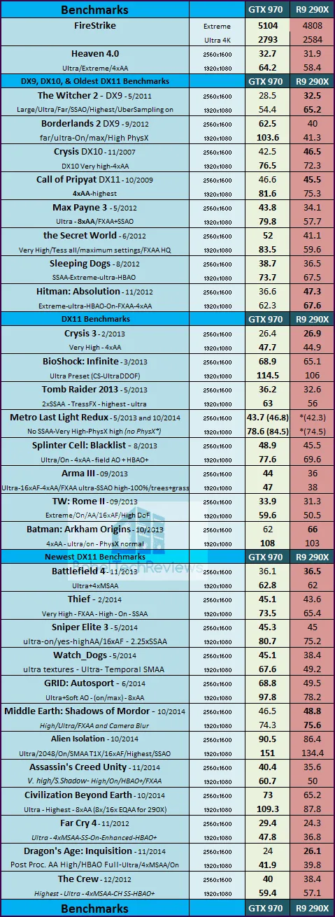
This looks to be a blowout in favor of the GTX 970. Nvidia has managed to surpass the performance of AMD’s flagship, the R9 290X with 4 cards – The TITAN Black, the GTX 980, the GTX 780 Ti, and now the GTX 970. Let’s now show our benchmark results of the GTX 970 versus the mildly overclocked PowerColor 290X PCS+ and adding GTX 970 EXOC and our user overclocked results, plus the GTX 980: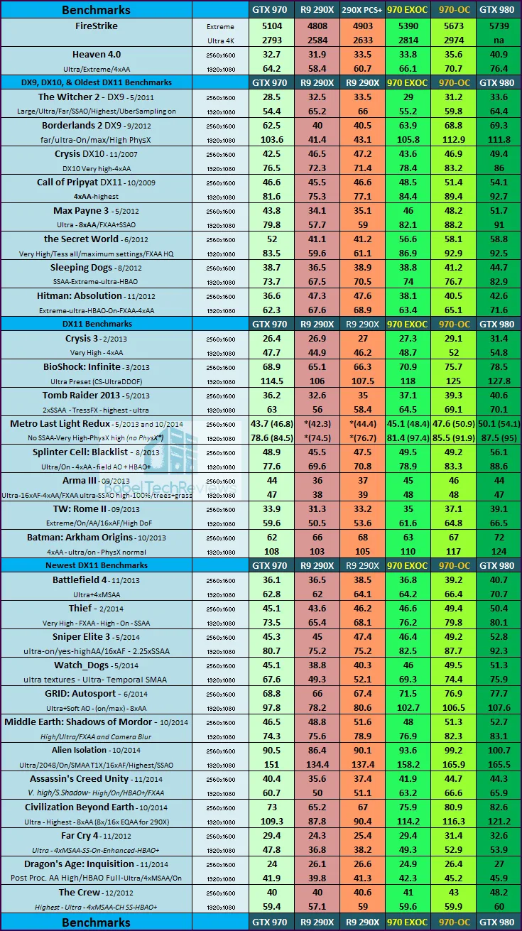
Well, the GTX 970 scales very well with overclocking although it doesn’t quite catch the stock GTX 980, and the extra 30MHz of the PowerColor’s 290X core speed doesn’t change anything. The GTX 970 even at stock clocks is faster than the typical aftermarket 290X.
Main Overall Summary chart
The main summary chart is what we call BTR’s “Big Picture” as it shows performance from the GTX 660 all the way up to the GTX 980 and R9 290X. Our Big Picture has recently changed to become smaller with our recent platform upgrade to i7-4790K and Z97 motherboard and it will grow larger again as more reviews are added.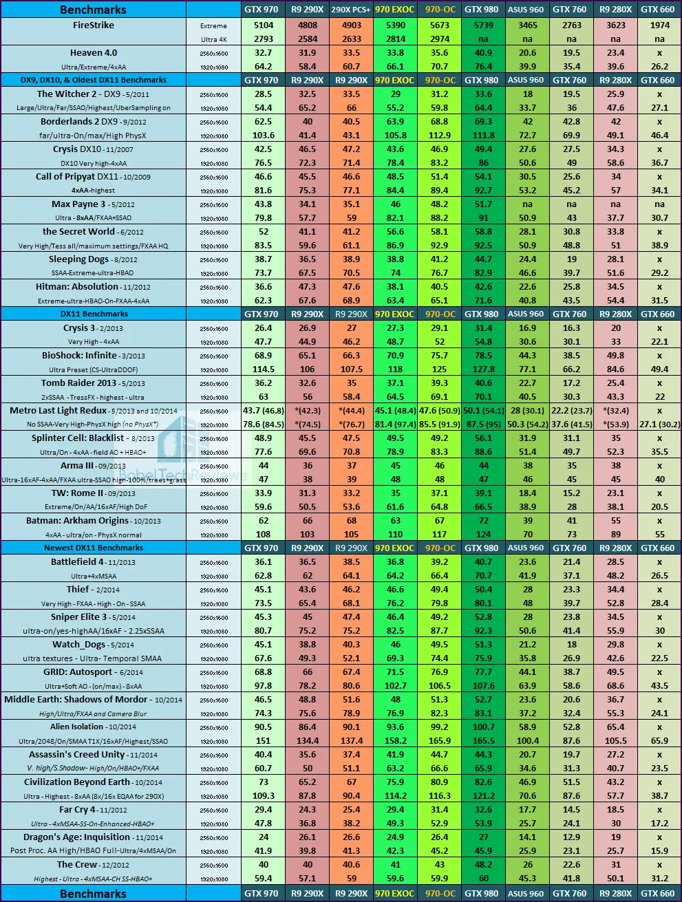
In most cases, the GALAX GTX 970 EXOC Black Editon is faster than the R9 290X even when it is overclocked by AMD’s partners, and it further pulls away in performance as it is further overclocked although it does not catch Nvidia’s flagship, the GTX 980.
Let’s head for our conclusion.
Conclusion
This has been quite an enjoyable exploration for us in evaluating our new GALAX GTX 970 EXOC Black Edition. It did extraordinarily well performance-wise comparing it to the reference versions of the R9 290X which do not throttle in cool ambient temperatures as we ran them. We are totally impressed with this cool-running GALAX card which is generally faster, cooler, more energy efficient, and quieter than its competitors in a similar price range.
We see good overclockability with excellent quietness at stock voltage and fan profile even when the GALAX GTX 970 EXOC Black Edition is overclocked beyond GALAX’ factory overclock and it scales well in performance. The GALAX GTX 970 EXOC Black Edition is as quiet or even quieter than the reference GTX 980 and yet it is perfectly suited for playing demanding games at maxed out settings at 1920×1080 and even at 2560×1600.
For its $349 price, the GALAX GTX 970 EXOC Black Edition fits in well with the other vendor mild to moderately overclocked GTX 970s. From our results, we can expect the GALAX GTX 970 EXOC Black Edition is also generally faster than any moderately factory overclocked R9 290X which are currently priced about the same as the GTX 970. For twenty dollars more than the reference GTX 970s cost, it makes sense to pick the GALAX GTX 970 EXOC Black Edition, while giving the gamer GALAX’ excellent support and a 3-year warranty.
If you are looking for a GTX 970 in the $350 price range, the GALAX GTX 970 EXOC Black Edition is an excellent choice.
Pros
- The GALAX GTX 970 EXOC Black Edition provides excellent performance for an overclocked $350 GTX 970 and generally beats the Radeon R9 290X at stock clocks and even beats factory overclocked cards in performance.
- Overclockability is excellent with the Galaxy-clocked +76MHz offset, and the further +90MHz we achieved without adjusting the voltage nor the fan profile. GPU Boost works as advertised and the +250MHz memory user overclock we achieved, also helps performance.
- The cooling design is quiet and efficient
- GALAX’ excellent 3 year warranty backed by 24/7 tech support.
Cons
- None, now that the full and correct specs of the GTX 970 are known, it is a very fast bang for buck card that beats AMD’s flagship.
The Verdict:
-
If you are buying a factory overclocked GTX 970, the GALAX GTX 970 EXOC Black Edition is an easy choice for $20 dollars more than the reference-clocked design. We feel it deserves BTR’s Editor’s Choice award since it is faster, cooler, quieter, and more energy efficient, than competing cards in its class and price range. It wins on every metric against the R9 290X and we expect that AMD will lower its prices further.
We do not know what the future will bring, but the GALAX GTX 970 EXOC Black Edition brings good value and a great performer to the GeForce Maxwell family. With great features like GameWorks and superb driver support from Nvidia, you can be assured of immersive gaming by picking this card for 1920×1080 or even 2560×1600.
If you currently game on an older generation video card, you will do yourself a big favor by upgrading. The move to a GALAX GTX 970 EXOC Black Edition will give you much higher performance. The competition is hot and AMD offers their own set of features including Eyefinity 2.0 and good price to performance cards as they cut the pricing on their cards to move them out.
Stay tuned, there is a lot coming from us at BTR including a performance evaluation of GTX 980 SLI versus R9 290X CrossFire where the overclocking gloves come off. And we will finally have our evaluation of Kingston’s HyperX Cloud gaming headset published this week.