The NVIDIA 2020 Editor’s Tech Day – Ampere Detailed
This editor was privileged to be invited to NVIDIA’s first ever online Editors Day yesterday for a deeper dive into Ampere and the upcoming RTX 3000 series details. We loved the fact that we didn’t have to travel, but we do miss the personal connections that face-to-face meetings and hands-on demos allow for. This brief summary is this editor’s personal experience with the event, with thanks to NVIDIA for inviting us on behalf of BTR.
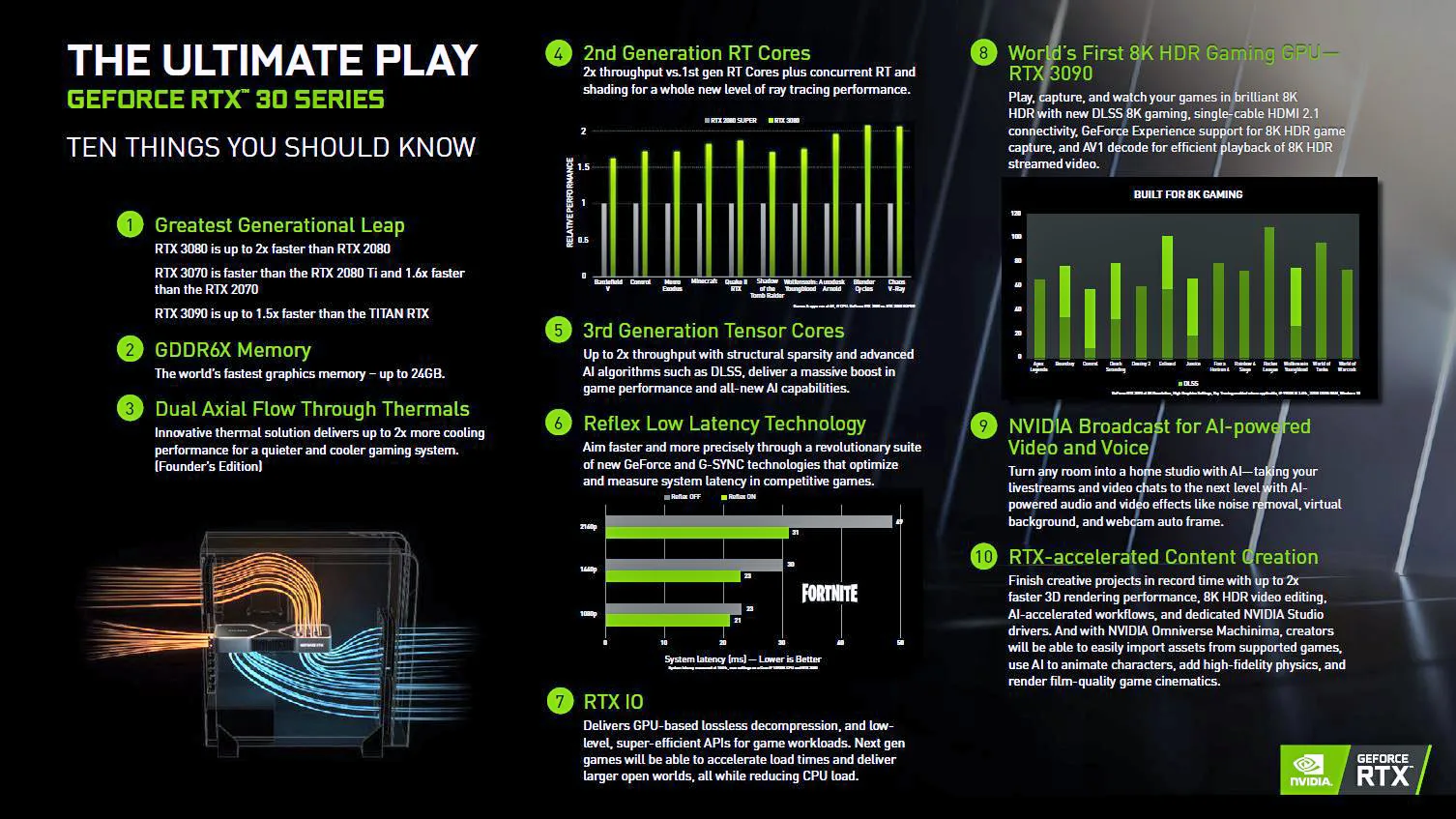
NVIDIA calls the Ampere generation “the “greatest generational leap” that they have ever made, with the upcoming RTX 3080 said to be up to two times faster than the RTX 2080 which was introduced 2 years ago. Here are the top ten things NVIDIA wants you to know before the launch reviews are released.
 Although there aren’t a lot of details beyond what NVIDIA’s CEO, Jen-Hsun (Jensen) Huang revealed, we are excited for what we learned, and will share what we can by including more details on the GeForce 30 Series from what we learned yesterday. And of course, we will bring you complete reviews – more detailed than ever before – as the NDAs end for each of the Ampere video cards in order: the RTX 3080, the RTX 3090, and the RTX 3070.
First of all, if you haven’t watched Jensen’s 39 minute official RTX 30 series launch , it offers a wealth of information.
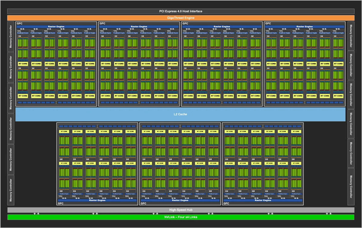
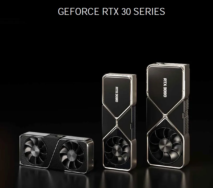
Let’s start by diving a bit deeper into the Ampere architecture and see what makes it such a large improvement over Turing. Below is the GA-102 chip diagram. It’s used for the RTX 5090 and it has all of its GPCs and the full 384-bit memory bandwidth, but with two SMs disabled. The RTX 3090 at $1499 is the only chip with NVLink for SLI. It’s a monster GPU with over 10 thousand CUDA cores, and equipped with 24GB of vRAM, it’s reported to be about 1.5 times faster than the $3000 TITAN RTX.
Session One – Architecture
Touted by NVIDIA as their largest generational leap, Ampere offers large increases in performance, memory bandwidth, and power efficiency over the current Turing architecture. It introduces new graphics features and technologies that confirm the PC as the ultimate platform for playing video games and for enjoying virtual reality, and they extend well beyond gaming to content creation and more.
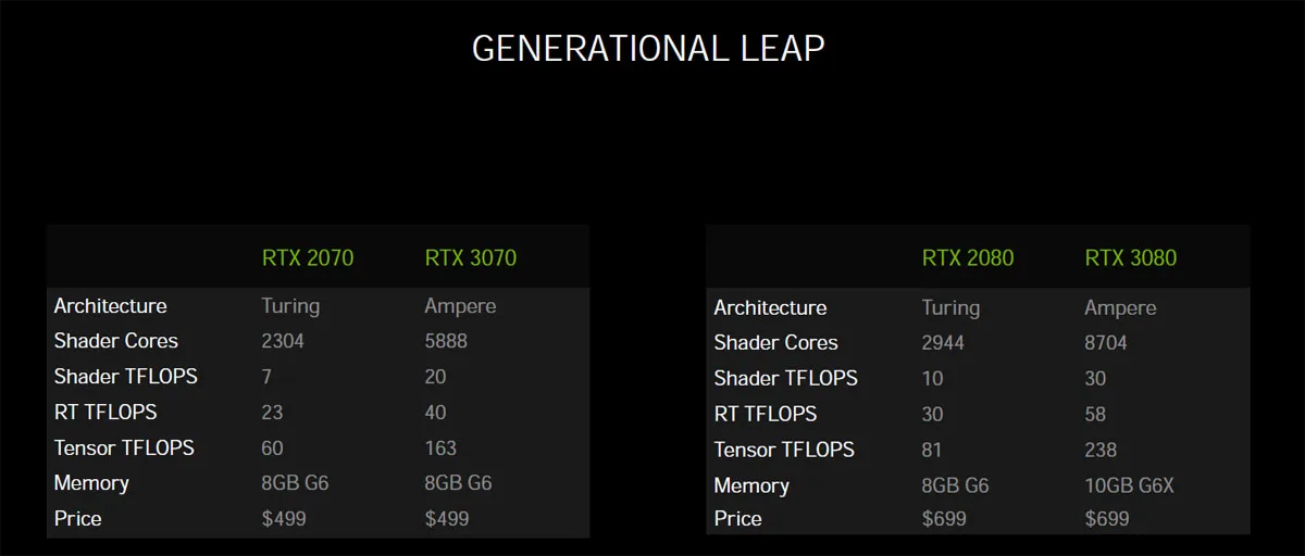
NVIDIA claims that the $699 RTX 3080 is up to two times faster than the RTX 2080 which launched at the same price. Although it is based on the same GA-102 GPU, compared with the RTX 3090, it uses a 320-bit wide memory interface and comes equipped with 10GB of vRAM.
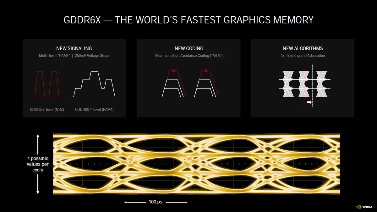
The memory used for the RTX 3080 and the RTX 3090 is the fastest GDDR6X custom Micron memory available. By using multi-level PAM4 signaling, it makes it possible to transmit four values per cycle instead of the usual off/on binary. However, since it is very difficult to process four signals instead of just two, new encoding is used that steps the voltage up or down with less dramatic swings.
We don’t know much yet about the upcoming $499 RTX 3070, but we guess it is based on GA-104 with 8GB of DDR6 – not DDR6X, and NVIDIA claims it will be faster than a GTX 1080 Ti. This translates to about 1.6 times faster than a RTX 2070 – which also launched at $499.
NVIDIA engineered the Ampere architecture to handle the demanding computing needs of technologies with an emphasis on ray tracing. In fact, as second generation RTX cards, Ampere is claimed to be 1.9 times more efficient than Turing and much more powerful for ray tracing.
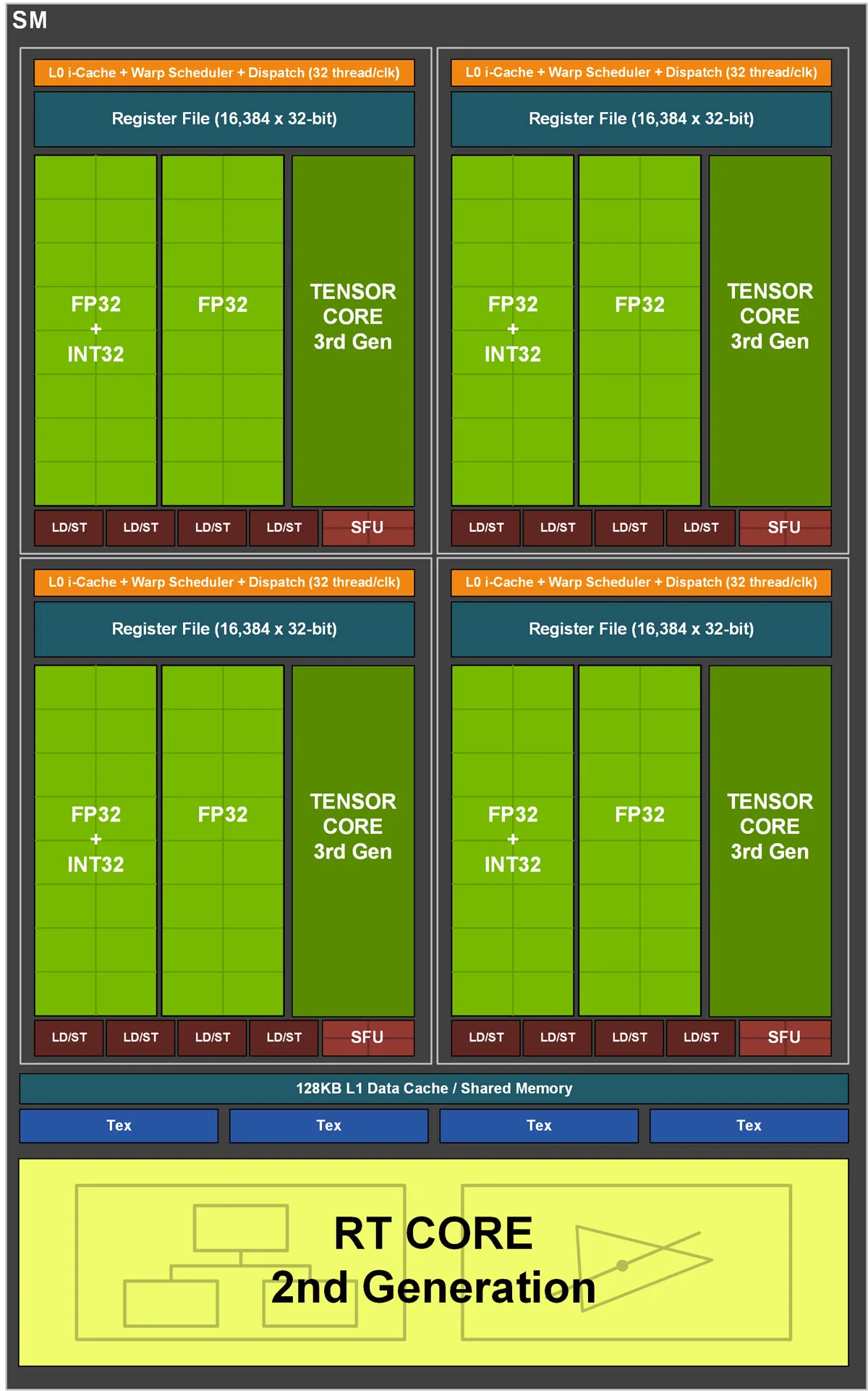
Turing’s SM – the basic block of the architecture – can deliver 11 FP32 TFLOPs, while the RT core delivers 34 TFLOPs, and the Tensor cores deliver 89 Tensor TFLOPs. It’s contrasted with the Ampere SM which delivers 30 FP32 TFLOPs, while the RT core delivers 58 TFLOPs, and the Tensor cores deliver 238 Tensor TFLOPs. So the core has been beefed up with a big emphasis on the Tensor cores which use AI/DeepLearning.
Although there are less Tensor cores per Ampere SM than Turing’s SM, they are much more powerful and its new datapath is about two times faster. The Ampere SM has double the L1 bandwidth of Turing with more capacity, and compute performance has approximately doubled. The Ampere ray tracing (RT) cores process triangles and Tensor cores run sparse matrix calculations at about double the speed over the first generation Turing SM.
NVIDIA has introduced other new hardware to the Ampere RT core that may use a temporal motion algorithm to speed up ray traversal by up to 8 times faster than with Turing.
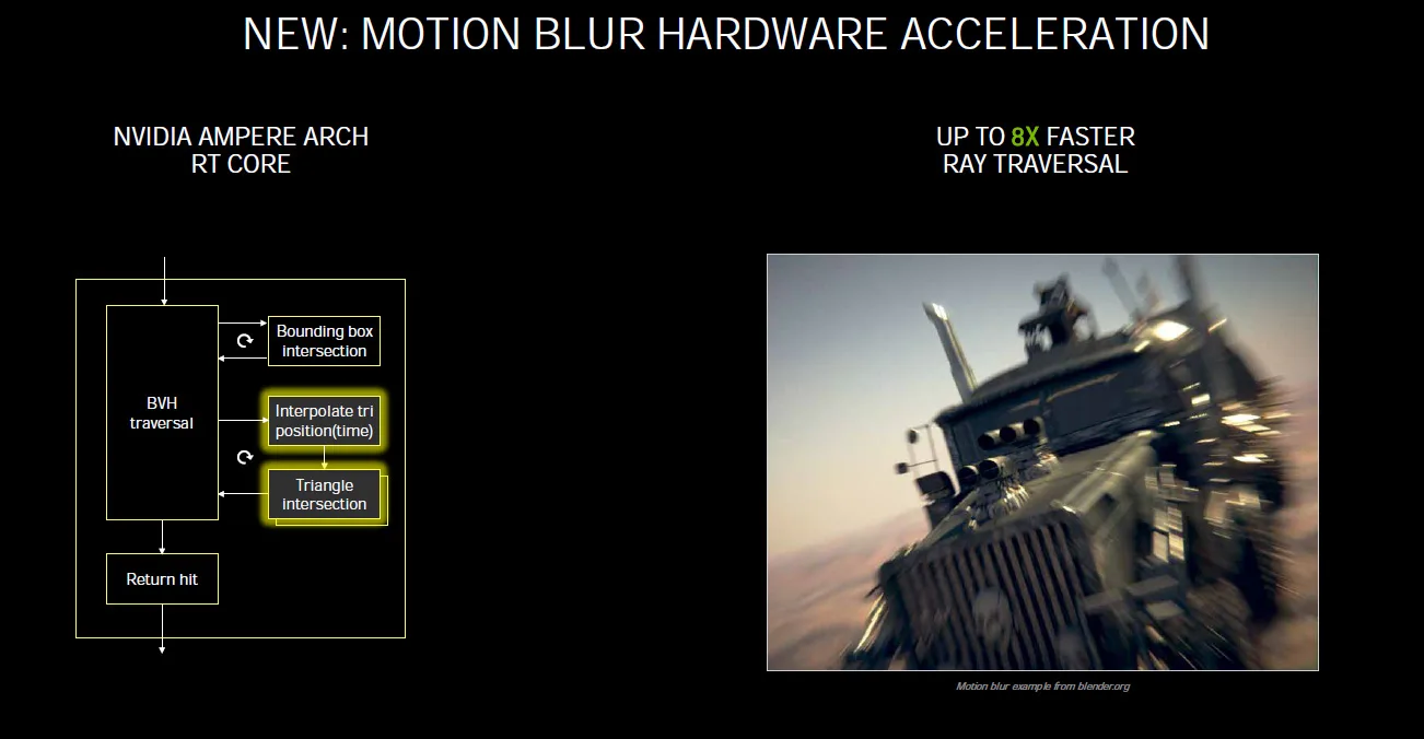
Ray tracing performance is up significantly as illustrated by NVIDIA’s image below: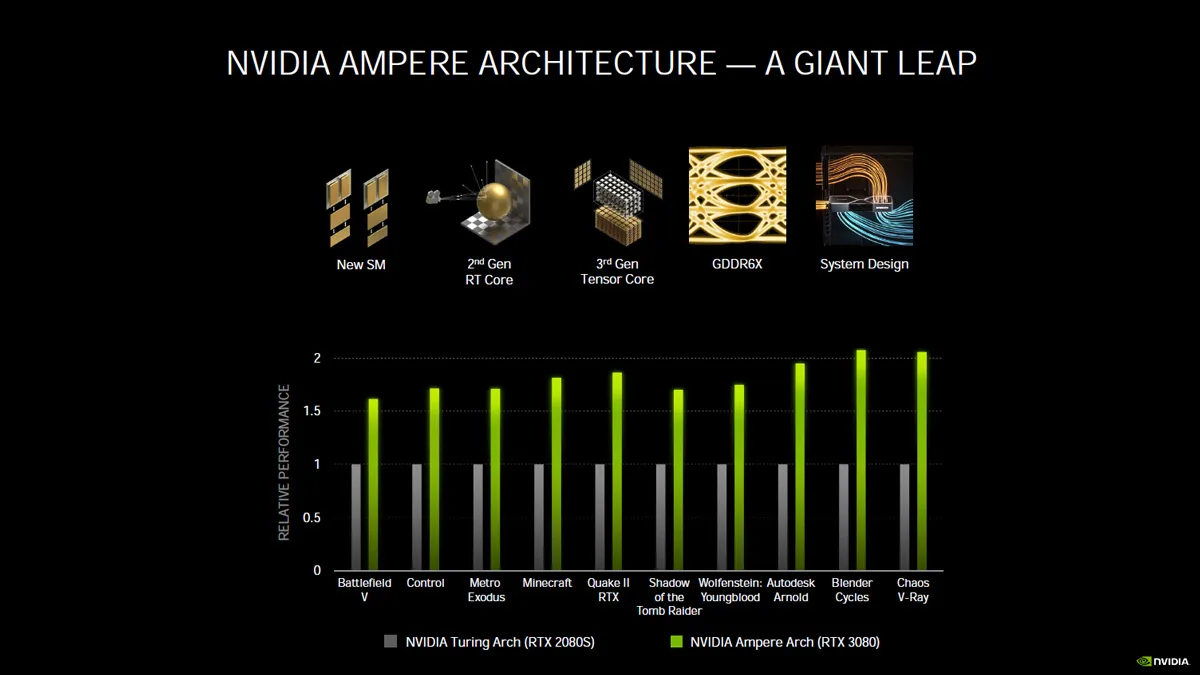
This means that 8K gaming is possible – if you can afford a $4000 Dell 8K display – and you will be able to drive it with a single HDMI 2.1 cable at 60Hz. With that same cable, you will be able to drive your new LG OLED 4K TV at 4K/120Hz. It is also has AV1 full hardware decode for 8K/60 real time processing of the latest and greatest videos.
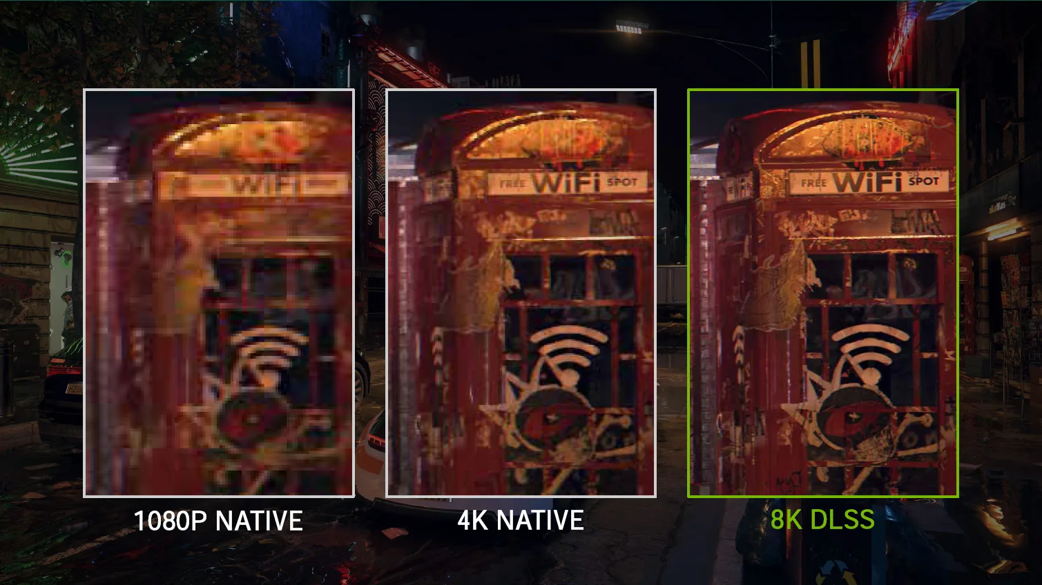
The new 8K DLSS 2.1, which is upscaled from a lower resolution, actually looks better than 4K native resolution from NVIDIA’s example taken from the upcoming Cyberpunk 2077 game above.
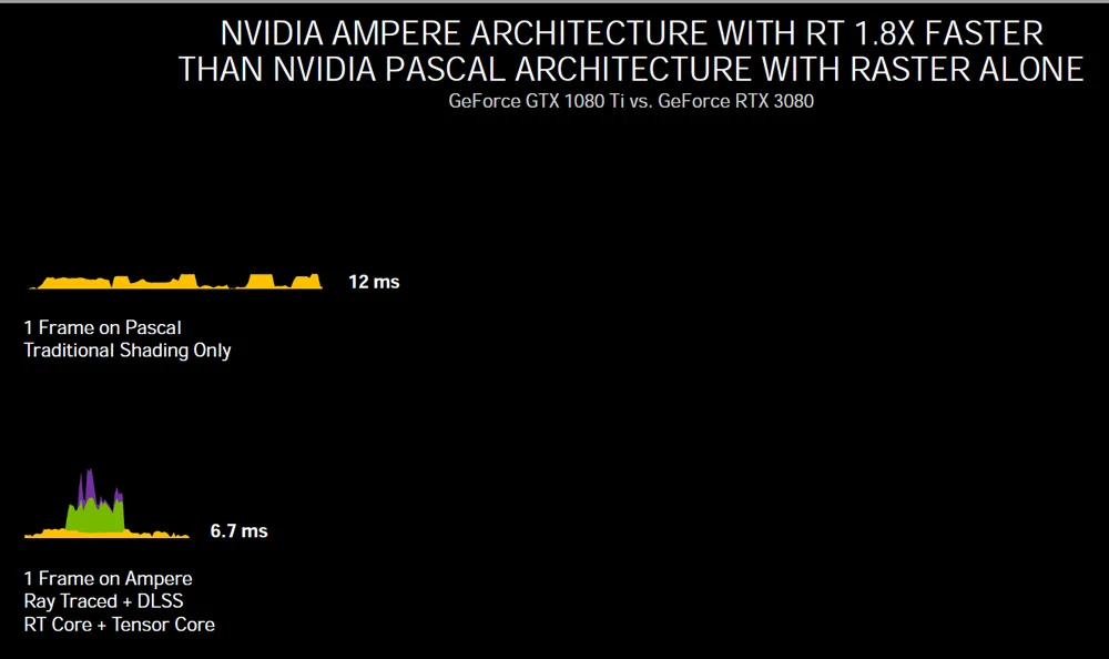
Perhaps more importantly for now, since most games are not ray traced, rasterization performance by Ampere is a giant leap over Pascal.
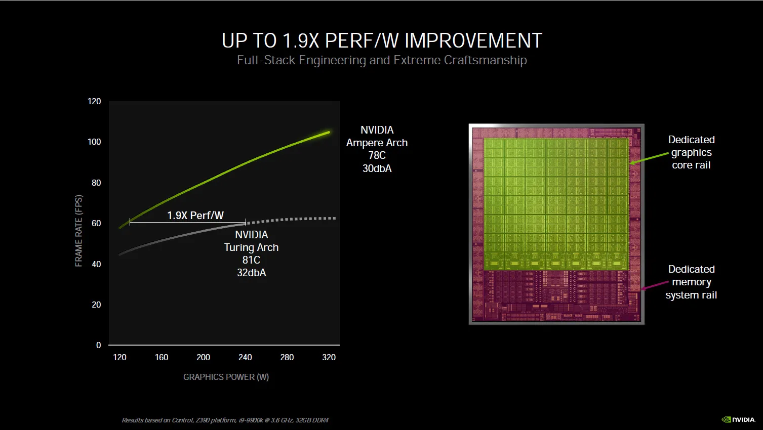
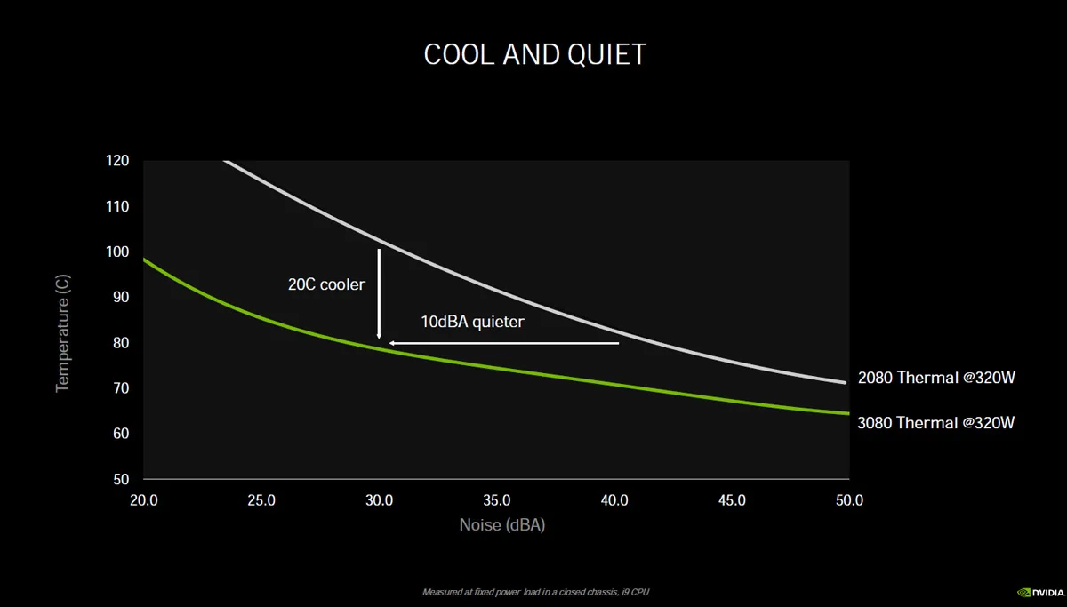
Performance per Watt has significantly improved according to NVIDIA’s slide, and it even uses a dedicated power rail for the memory. This results in a cooler running Ampere architecture compared with Turing. Overclocking may be improved and we can’t wait to bring you those results!
Finally, huge new open world games bring challenges to IO and storage. Currently game developers target the HDD as their lowest common denominator. This may well change with the next generation consoles. No gamer like to wait … and wait … and wait as a game or game level loads. It wrecks immersion, so many gamers use SSD storage and especially NVMe2 SSDs as we do for all of our games. Yet waiting is a fact of life for gamers using even the fastest NVMe SSD on PCIe4.
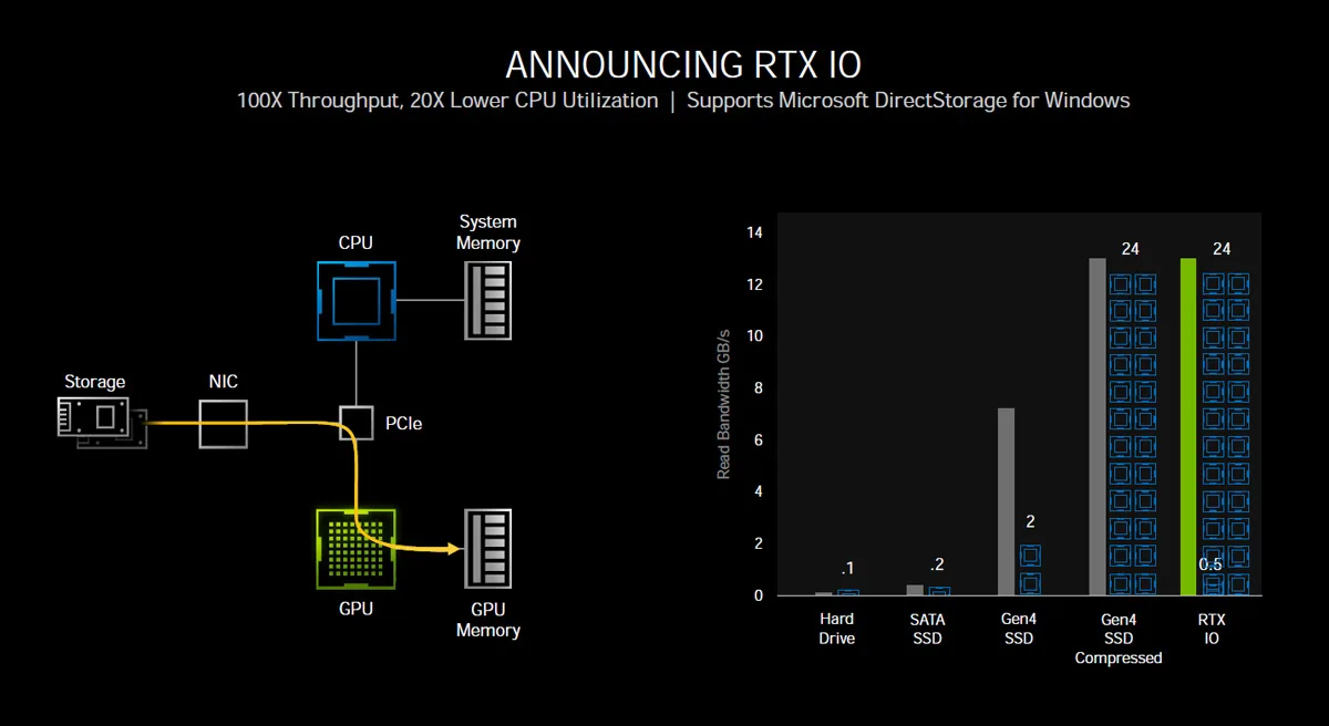
100GB games are becoming more common, and developers depend on the CPU as they generally use uncompressed data now. However, since the amount of streaming data is huge, and when compression becomes necessary, it strains CPU resources to their breaking point so that even a 24-core Threadripper becomes saturated. So NVIDIA introduced NVMe GPU decompression.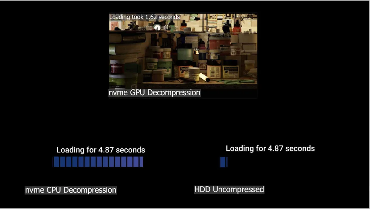
Loading the path traced Marble demo took 1.6 seconds using NVMe/GPU decompression while using NVMe CPU decompression took 4.87 seconds. A hard drive takes over a minute to load the same scene.
Session Two – The Ampere Products
The RTX 3080 and the RTX 3090 use an innovative cooling system so they can stay cool in a typical PC chassis where the airflow enters the front and exits the rear. NVIDIA has modeled what they consider to be an optimum airflow.
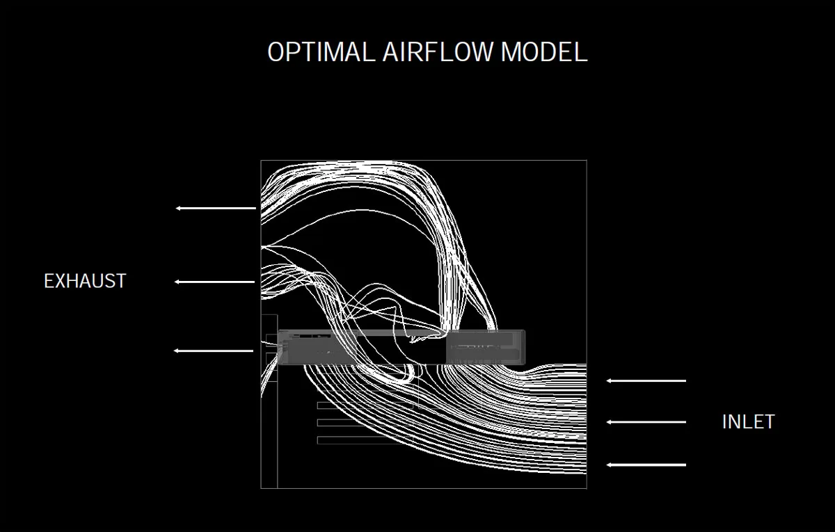 To achieve this optimum airflow, NVIDIA has engineered their top cards’ cooling very differently than ever before.
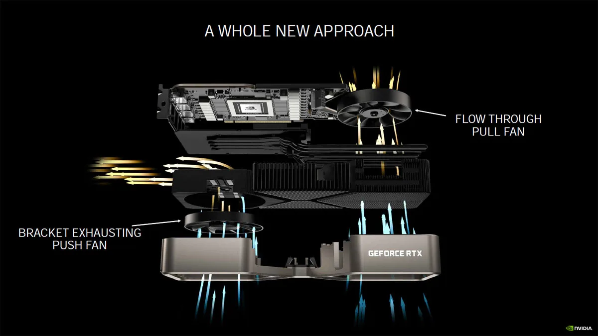
This evidently results in a much cooler-running GPU, although in some very small form factor cases where airflow is compromised, the hot air may warm the CPU.
Finally, this sums up NVIDIA’s generational leap.
There is much more that was covered in-depth including RTXGI – fully enabled Global Illumination with a minimal performance hit – but we will cover it in our launch review of the RTX 3080.
Session Three – eSports
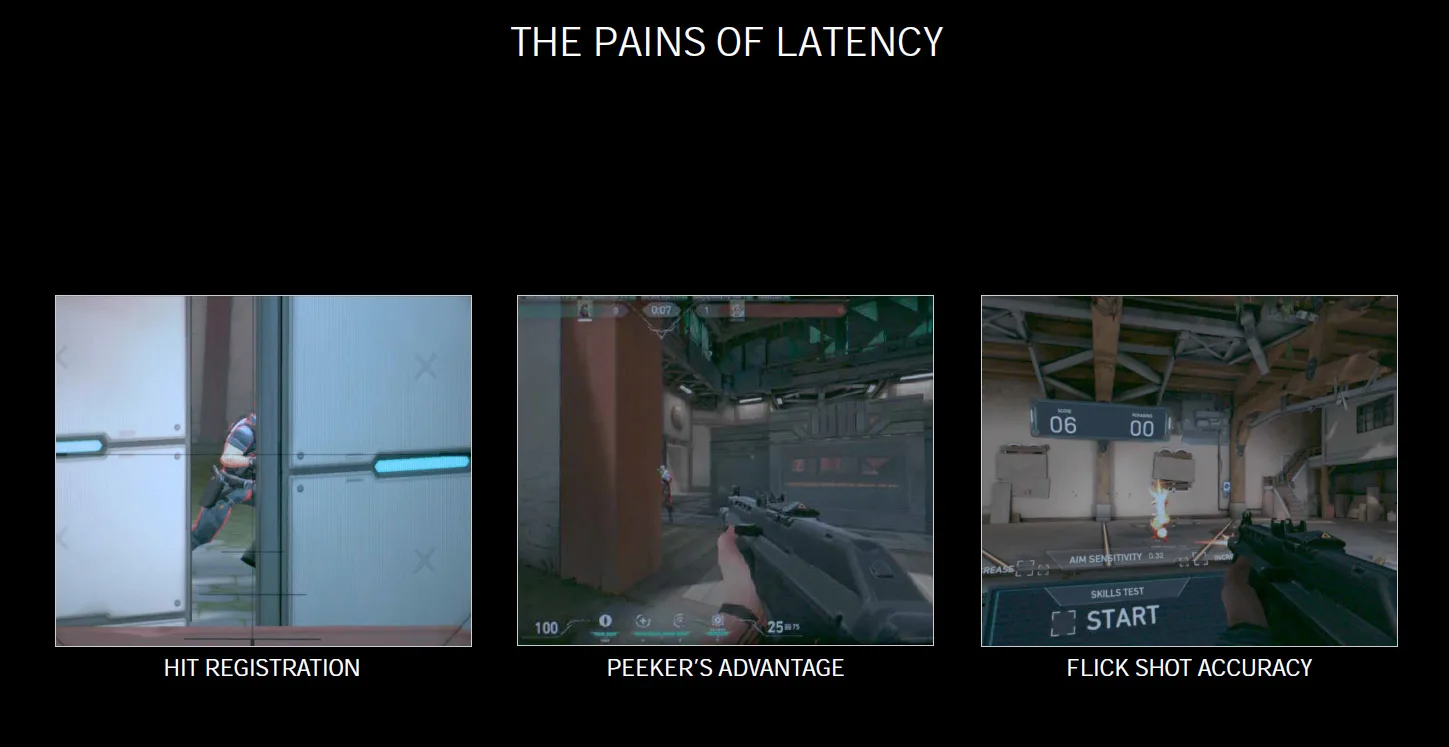
eSports is fast becoming the most popular competitive sport in the world and NVIDIA has been careful to address the needs of this huge group of players. Latency is a big problem that many online gamers just accept, and often they attribute it to ‘ping’ or to network latency without considering that their own PC’s end-to-end latency is critical to their aim accuracy for success.
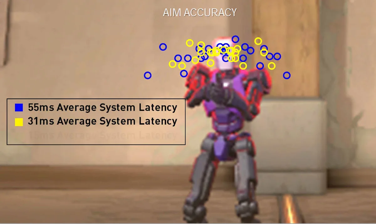
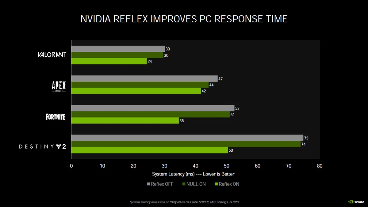
Enter NVIDIA’s Reflex technology which reduces the backpressure on the CPU, reduces the render queue to zero, and boosts GPU clocks, and gives some pretty impressive results.
BTR recently purchased a SAMSUNG LC27G75TQSNXZA 27? 2560 x 1440 240Hz 1ms G-SYNC HDR600 Monitor, and we can certainly tell the difference between a 240Hz refresh rate and a 120Hz refresh rate. But NVIDIA has new displays on the way that feature 360Hz. For online competitors, it may make the difference between winning and losing.
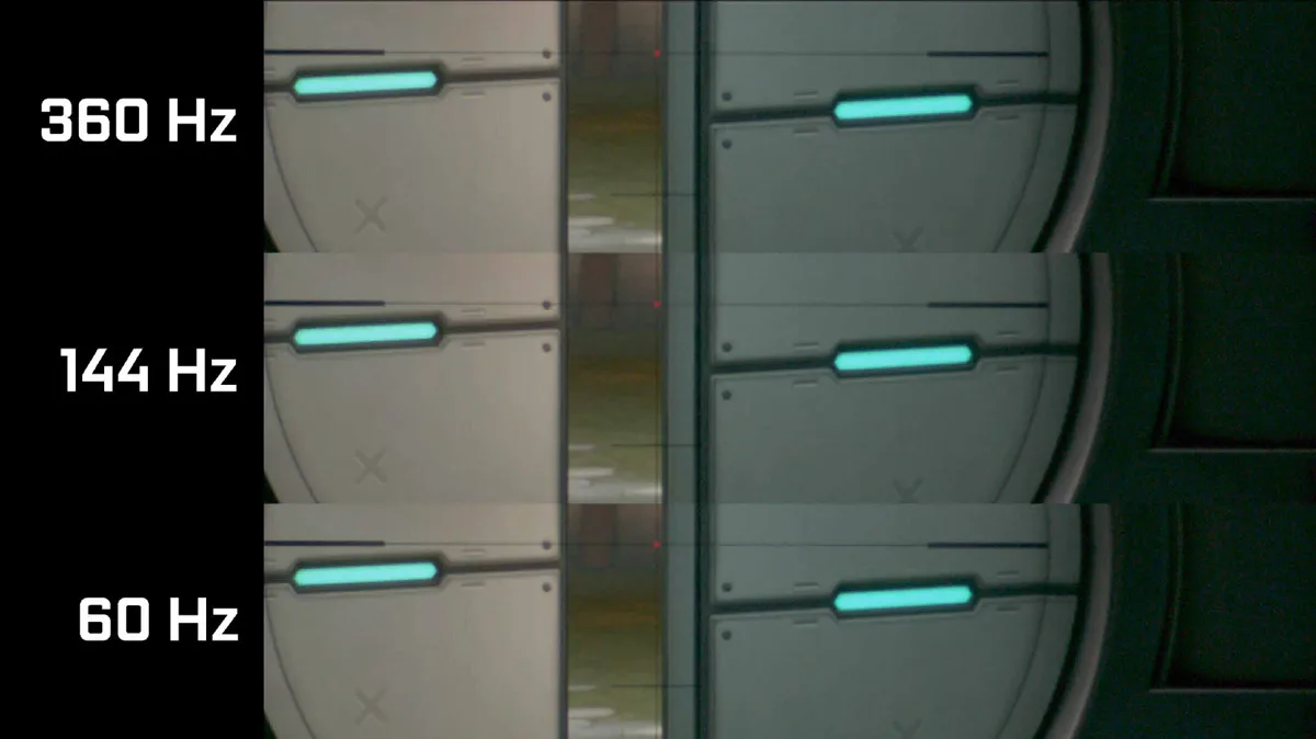
These new upcoming displays by NVIDIA partners include ACER, Alienware, ASUS, and MSI.
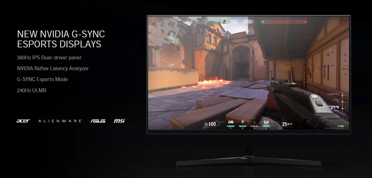
These G-SYNC displays include a built in system end-to-end latency analyzer in real time using a compatible mouse that integrates with a new GeForce performance tool that also automatically optimizes system latency. 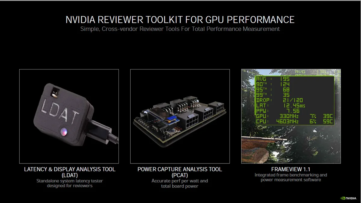
A few reviewers have received this kit, but we won’t say more about it now. LDAT simplifies latency and display analysis – without having to spend many thousands of dollars for time-consuming and complicated equipment using a super-high speed camera. And PCAT measures and analyses the power draw of any video card. Stay tuned to BTR for much more on LDAT and PCAT!
Session Four – Creators
BTR focuses on gaming although we realize that creators use GPUs for rendering and for content creation. We only dabble in Blender, and we use its benchmark to compare CPU performance and GPU performance.
Creators will love the gigantic 24GB of vRAM that comes with the RTX 3090.
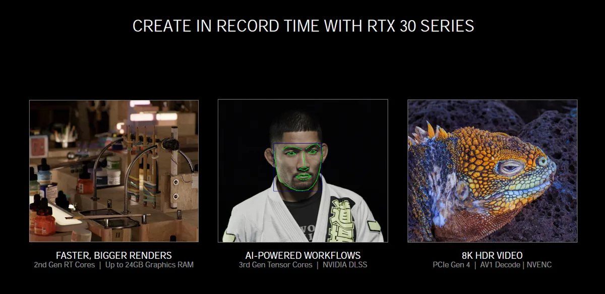
The RTX 3080 renders ray tracing workloads twice as fast as the RTX 2080, and Blender speeds up by a factor of 5X on motion blur rendering. Even DLSS has come to creative apps! And NVIDIA’s Omniverse Machinima is perfectly suited for using video games for story telling.

Conclusion
NVIDIA has created the most exciting product launch that we can remember since we first covered NVISION 08. Stay tuned to BTR for the launch reviews and for the latest news!
Happy Gaming!